> What is a V-groove color tunable LED, and how does it improve color
coverage in display technologies?

A V-groove color tunable LED refers to a specific structure used in LED displays
that combines the benefits of both vertical and lateral LEDs. It achieves this
by utilizing semi-polar facets within each V-groove, which facilitate efficient
carrier confinement and minimize non-radiative recombination. This leads to an
increase in red to blue color ratio while also improving overall luminance
efficiency. As a result, V-groove color tunable LEDs offer enhanced color
coverage with high brightness levels for various display applications.

> Tell me about chemically amplified resist

CAR is a flowable photoresist based on an organic nitrile compound dissolved
in a solvent system, which contains a very small percentage of a
tetrazole-containing monomer and a catalyst. during exposure to UV light,
this monomer splits into ammonia and a ketone byproduct while the catalyst
gets activated. at elevated temperatures, the tetrazole groups undergo a
chain reaction, causing the resist material to crosslink, forming insoluble
polymer networks that prevent further development with solvents or alkaline
solutions. the amount of crosslinking is proportional to the dose received
during exposure, allowing for selective removal during the developing process.
CAR offers several advantages such as better resolution due to its very low dark
resistivity, excellent flatness, and improved sensitivity compared to conventional
i-Line lithography processes.

> Which metals are typically used for making an ohmic contact to p-GaN,
and how does their thickness affect resistivity?

Commonly employed metals like Ni and Au can be utilized as p-type metalization
layers to establish efficient ohmic contacts with p-GaN regions in semiconductor
devices. The resistance offered by these layers depends on their respective
thicknesses; for instance, a thicker Ni layer would result in higher resistivity
compared to thinner layers. Consequently, optimizing the thickness ratios between
these metals is crucial for achieving desirable contact resistances and ensuring
reliable electrical performance within the circuits.

> Can you tell me about the use of AZ400K to form GaN nanowires?

Yes, AZ400K is a popular choice as a wet etch chemical solution for selectively
forming Gallium Nitride (GaN) nanowires due to its ability to etch GaN
anisotropically (along specific crystallographic planes) while leaving other
surfaces untouched. This leads to the formation of perfectly vertical wires with
minimal sidewall roughness or damage, making it an essential component in
fabricating devices like light emitting diodes (LEDs) or high electron mobility
transistors (HEMTs). The exact mechanism behind this selective etching behavior
is not fully understood but believed to be related to differences in surface energy
and polarity between various crystal planes of GaN.

> What temperatures are commonly used in the wet etching of GaN in AZ400K?

The temperature control is a crucial parameter during the GaN nanowire etching
process as it can significantly impact both selectivity and etch rate properties.
Commonly employed temperatures for AZ400K solution fall within the range of 40-80C
degrees Celsius, depending on application requirements and desired wire dimensions
or device structures. Higher temperatures generally lead to faster etching rates but
may also increase the likelihood of non-uniformity in diameter or sidewall damage
due to thermodynamic fluctuations. Conversely, lower temperatures result in slower
etch rates but improve selectivity and reduce the occurrence of unwanted surface
roughness or defects that could degrade device performance.

> How does the refractive index change with the density and quality of an oxide?

The refractive index is directly influenced by both the material's physical properties
(density) and its chemical composition (quality). A higher density generally leads to
a greater refractive index, while better-quality materials exhibit more consistent and
accurate refraction across various wavelengths. Therefore, ensuring proper control over
oxide deposition conditions such as temperature, pressure, and reactor chemistry is
essential for achieving desirable refractive indices in devices fabricated on top.
Semiconductor Trained AI
Developed a locally-run AI system trained on a comprehensive dataset of academic papers I've read and personal notebooks.

AI embodies a burgeoning technology that holds substantial promise in enhancing data analysis and comprehension. At the core of these large language models propelling the AI momentum are vast troves of data that shape the generated responses. Despite its ubiquity, semiconductor manufacturing often remains in the background, rendering it a more elusive field for individuals to delve into. Consequently, data in this domain can be challenging to acquire, reflecting a more closed nature of the technology.
With this backdrop, employing a large language model on semiconductor data could prove invaluable. Despite the moniker "OpenAI," popular platforms like "ChatGPT" are proprietary, offering scant data security measures. Conversely, there are emerging open-source models which can be run locally. Mistral has emerged as a key open-source model which rivals the likes of ChatGPT, with great performance and size benefits from its 7B model. However, all models are limited in their knowledge of semiconductor physics, processing, and nuances.
In this endeavor, Low-Rank Adaptation (LoRA) of a large language model (LLM) can be performed in order to tune the existing Mistral 7B model on a semiconductor dataset. LoRA fine-tuning provides a very cost-effective way to train an existing model by adapting the lower layers and keeping the higher layers frozen. This approach helps ensure that the fine-tuning provides an understanding of the new data, while also retaining base knowledge and understanding.
To derive the most insightful output, data relevant to my research areas is supplied. Consequently, I have digitized hundreds of papers alongside my annotations, as well as presentations, lectures, and notes from my undergraduate through PhD studies. I have maintained a digital archive as I believe it is immensely beneficial in today's landscape as it facilitates easy data access, ensures security, and promotes data longevity. These datasets are meticulously organized locally, where initially over 45,000 data points are generated for training.
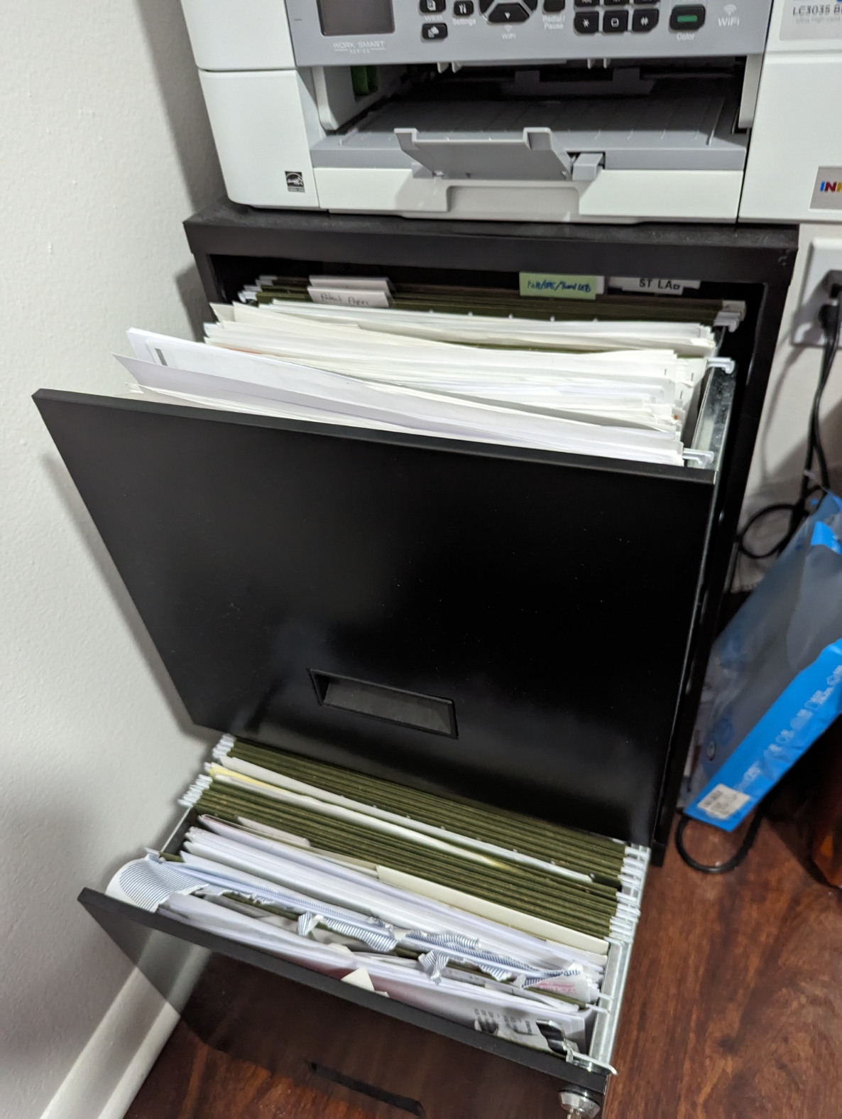
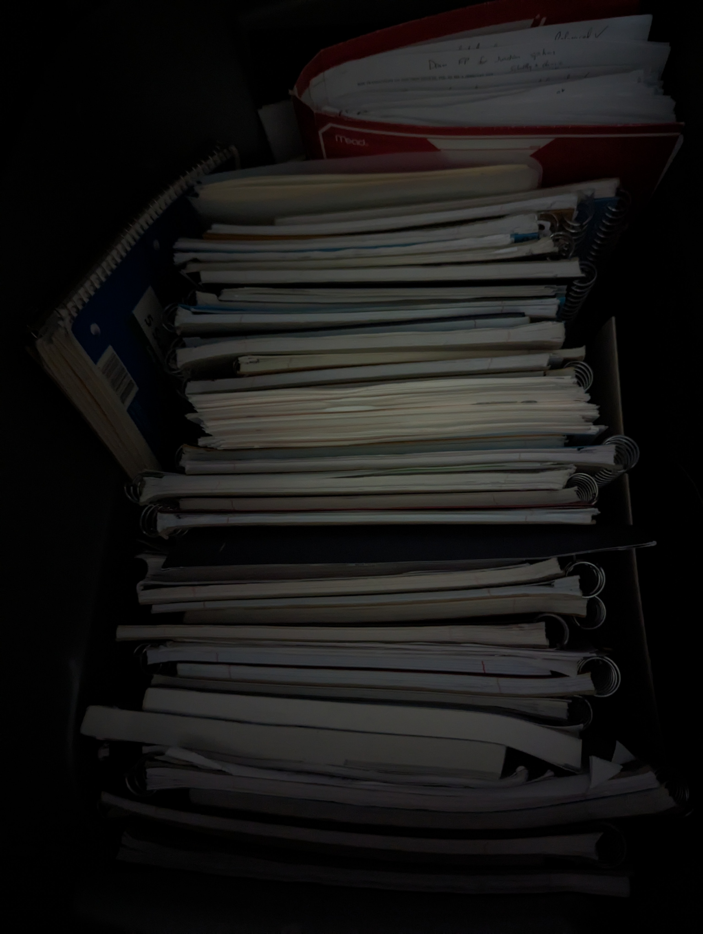
Cabinet with some scientific papers read and annotated (left), and notebooks I have scanned in (right)
The LoRA fine-tuning is done locally on a GTX 4090 graphics card, going through several epochs, totaling over 75 hours. The adapter output from training is converted over to the versatile ‘gguf’ format with an intial size of ~14GB, and then 4-bit quantized to be only 4GB. The final model can be loaded into the system’s RAM and run on the CPU or in VRAM and run on the GPU. Where the model performs best with the parallel processing provided by a GPU, giving near instantaneous results to inquiries.
The open source Ollama software it utilized to locally run the model, along with the Ollama web-ui which provides a ‘ChatGPT’ like interface on my local network to interact with the model. The advantage of the local web-ui is that any device on my network can utilize the hardware power of a desktop computer to run the model, such that an iPhone can readily interface with the model for questions.
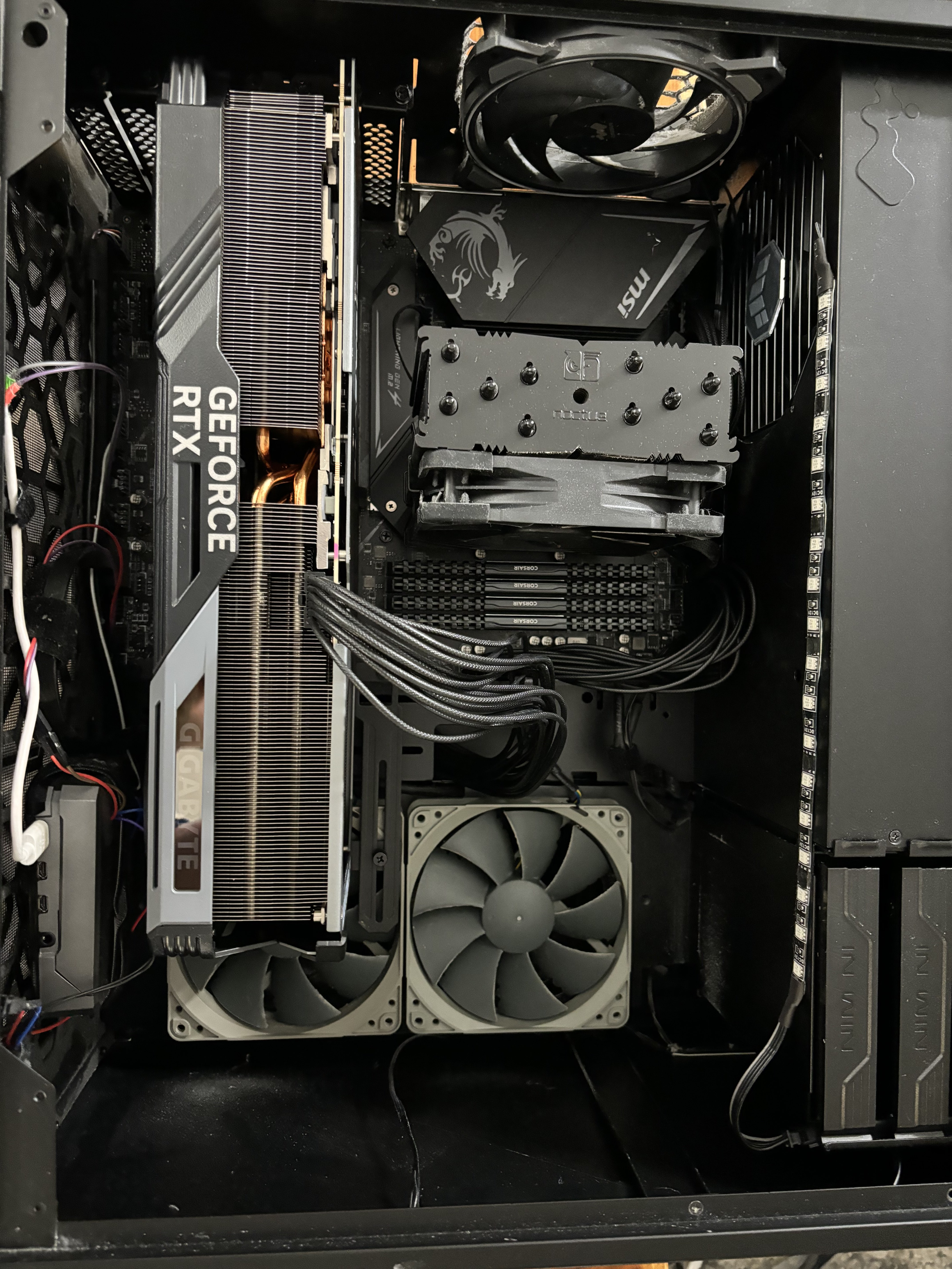

Desktop computer for training and running the model (left), and Ollama web-ui running the trained model (right)
Below are illustrative question and responses generated by the model.
Example Questions
Going forward I plan to expand the scope of the data and continue to refine the model. Possessing a tailored AI as a semiconductor engineer today is an invaluable asset, immensely aiding in problem-solving. Harnessing emerging technologies to address contemporary challenges is pivotal in navigating the complex landscape of the semiconductor industry today.