Home Cleanroom
Creation of home cleanroom for the utilization of semiconductor device research and fabrication.

Having a cleanroom is critical to achieving any level of semiconductor fabrication. There are around one million particles larger than half a micron in very cubic foot of office air. When trying to fabricate devices at the near nanoscale, just one such particle can kill the entire device. Furthermore, there are a multiple of fabrication steps involved which require the wafer to be exposed for a period to ambient air, making the particle issue a key impediment to semiconductor device development.
With the goal of internal device development, where the focus is on isolated device instead of grand scale integrated systems, I had initially thought that I could leverage a higher number of isolated devices to my advantage to have some level of statistic yield while still working in the room ambient. While this may be theoretically be possible, in developmental devices and processes rework is often a necessity. It was found that particle build-up overtime would be too big an impediment, despite the implementation of cleaning steps.
Conventional cleanrooms can cost millions of dollars with specialty flooring, roofing, walls, furniture, etc. all geared towards low particle counts. However, a key goal of mine is to have a compact design which is incompatible with this. Instead, there are some more modular options available in a variety of form factors.
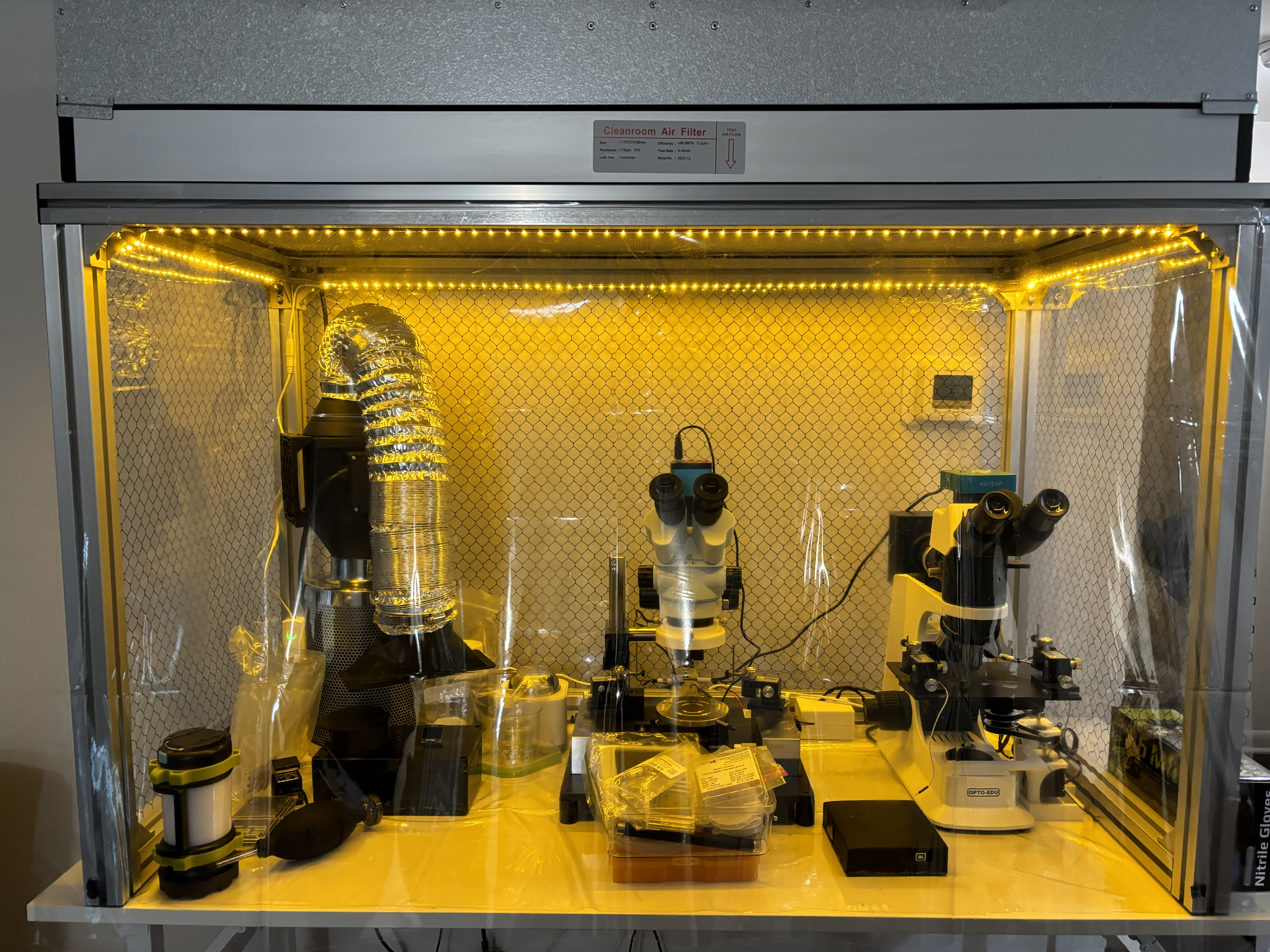
I settled on a type of cleanroom hood system that I could put a desk. The system had an aluminum extrusion frame which could be assembled, a large HEPA filter, a fan on top of the HEPA filter, and PVC film walls which had a conductive coating patterned on them to minimize electrostatics. The unit was rated to create a class 100 or better environment under the hood.
To add to the system, I had purchased an additional PVC film to line the bottom of the table, and then made a PVC film curtain on the open end. Lighting is a key concern while working under the hood as photoresist is sensitive to the shorter blue emission from conventional lighting. In an commercial foundry labs make use of yellow emission typically though added filters to available lighting such as CFL bulbs. For lighting I had purchased a yellow LED light strip, verifying with a spectrometer that the emission was ~580nm and there was no blue light leakage, then installed that under the hood.
Under the hood I have placed critical components for fabrication such as an optical microscope used for sub-micron lithography and optical characterization, a small probe station, then a custom-built spin-coater placed under a fume extractor along with a hot plate.
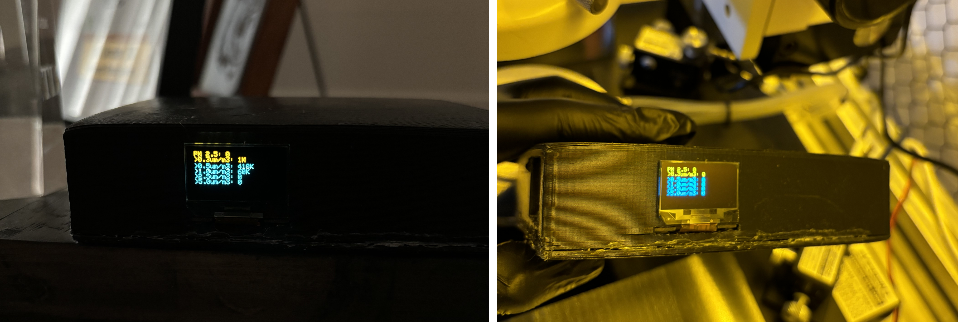
The comparative and practical results have been dramatically improved over previous work. There has been no evidence of particle deposition from the air to the sample surface while I am processing them or leaving them out in the open. To quantify this improvement, I leveraged a laser-based particle counter I had previously built. The particle counter gives a PM 2.5 reading as well as lists the number of particles greater than a set of sizes which include >0.3um/m3, >0.5um/m3, >1.3um/m3, >2.5um/m3, and >5um/m3. Depending on what I am doing and where the particle counter is located generally there are over 1M particles greater than 0.3um in size in each cubic meter of air. By comparison under the cleanroom hood the particle counter bottomed out and was not able to pick up anything. The nice aspect of a hood as well is that any particles which are generated from any of the items present get flushed out due to the constant laminar flow of the air, providing an excellent cleanroom environment.

I plan to do all further device level work leveraging this cleanroom hood environment, only taking samples out for processing in external tools like the reactive ion etcher, with operates under vacuum.