World's Smallest Resume
Patterned resume down to the near nanoscale at home through the use of microscope lithography.

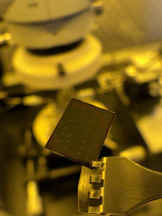
In order to run some calibration work on my microscope lithography system I thought it would be a good idea to engineer and test a pattern which contained some small feature size in order to judge aspects of emission uniformity, optimum focus, and exposure dose.
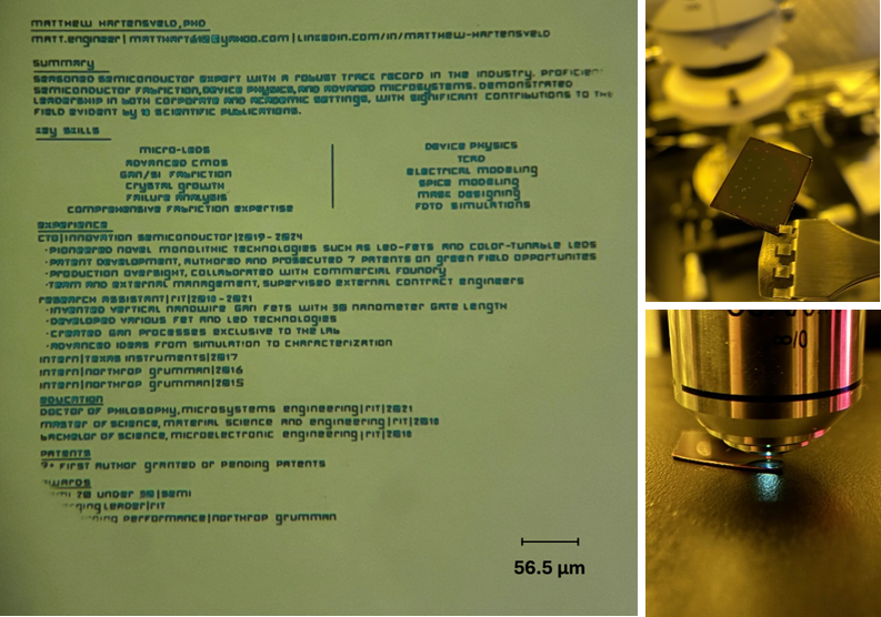
On that note I designed this test pattern making use of a compressed version of my resume, making use of similar sized lines to compose each letter. The mask is printed on mylar films to be readily integrated with the microscope, similar in essence to conventional steppers.
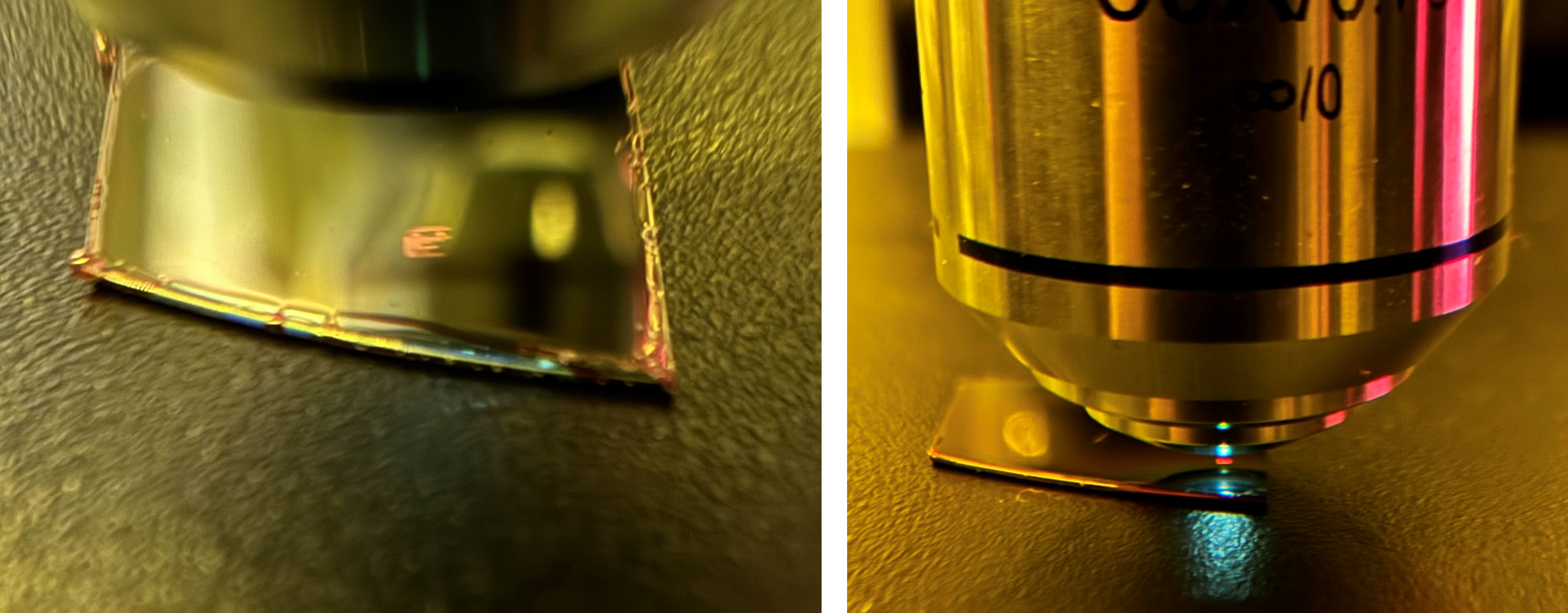
Depending on the objective in use there is a different level of magnification which is applied (certainly as well as NA as can be also seen from the objective spacing). Below are two images of the 20x and 50x exposing a silicon piece coated in photoresist. The level of zoom isn’t 1:1 as there is some diffraction and spreading of the resulting mask pattern in this setup. For example, the 50x objective results in a 20x reduction from the mask to sample surface.

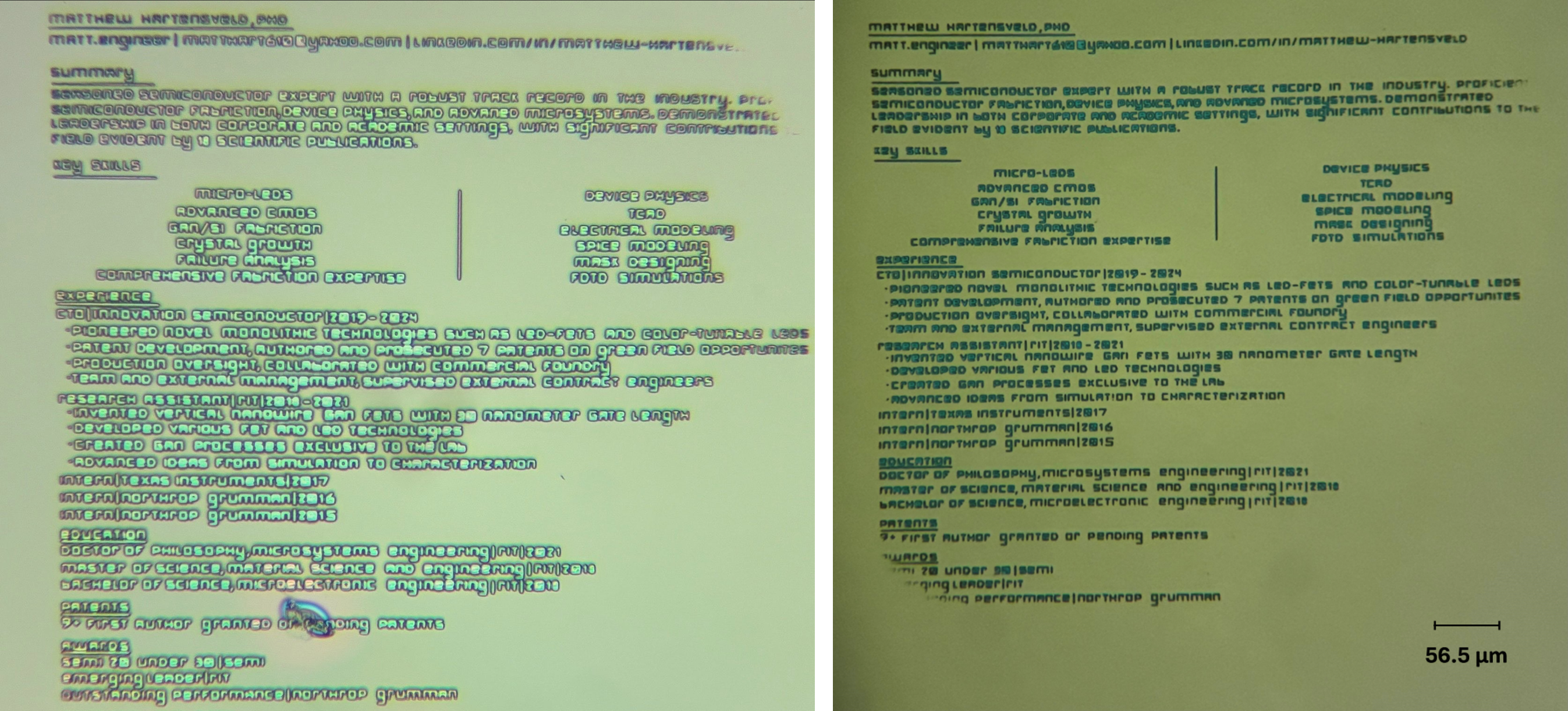
At 50x the mask design was engineered to have each line resulting in a width of only 1 um. Where the total pattern was ~370 um x ~410 um. These resolutions are conventionally produced with tools which can cost upwards of several hundred thousand dollars, where I don’t think anyone else has been crazy enough to pattern their resume with such a tool, let alone in a home environment.

The source did require some level of optimization. Initial trials showed a bright spot such that the center of the pattern was overexposed compared to the edges which were underexposed. This was corrected with an custom filter I had to engineer to minimize light in that spot to a more balanced level. Interestingly I did try to play with the kohler illumination setup, though did not have much success with that approach, perhaps it is more fundamentally limited by the use of a non-ideal point source with the Lambertian pattern of an LED.
The end result though I believe came out great! The only slight issue is that I am still a bit limited by field size as can be seen as the bottom left corner is a bit cut-off, however that is the compromise with such a system.

Future work is planned in order to etch these patterns into an oxide layer, and also to perform metal lift-off (when paired with LOR) for a nice contrast.
If you would be interested in having one of these dies, contact me!